Multi-cycle CPU
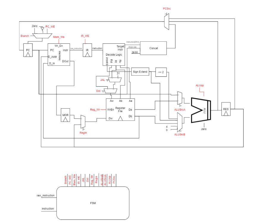
In Olin College’s Computer Architecture class, another peer and I designed and implemented a multi-cycle CPU in Verilog and wrote and tested Assembly programs to test it. As opposed to a single-cycle CPU which executes one instruction per clock cycle, the multi-cycle CPU takes a different number of clock cycles to execute different instructions. In order to perform instructions correctly, we also implemented a finite state machine (FSM) to guide the hardwre. The schematic for the CPU can be found below:
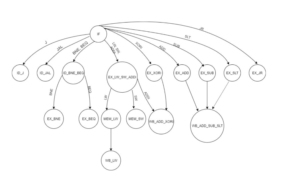
Note that we also designed and implemented the arithmatic logic unit (ALU) and register file components. When an instruction is initiated it follows the control signals of the various components in the CPU schematic (shown in red) are altered depending on the state. Then, the next state is determined by the current state and the instruction being executed. The FSM diagram can be seen below:
Consider a branch equals (BEQ) instruction. The CPU would begin in the instruction fetch (IF) state, move into the correct instruction decode state (ID_BNE_BEQ) which is the same for BEQ and branch not equal (BNE). Lastly, it would move into the correct execution state (EX_BEQ). At in each of these states, control signals are set so that the CPU is correctly carrying out the instruction. Every “leaf” of the “tree” FSM diagram leads back to the IF state to fetch the next instruction.

